


|
Let's make pretty printed circuit boards! Q: What makes a PCB pretty? The definition I'm going with for this thread is that if any consideration was taken regarding the PCB's appearance outside of practical electrical/mechanical considerations, it's a pretty PCB. Making an exact replica of an S-100 board based on a scan of the original PCB? Pretty PCB. Making a PCB with circuits in the shape of your favorite baked goods? Pretty PCB. Making an electronic business card with a functioning circuit that also looks like your face? You'd better believe that's a pretty PCB. Q: How do I make a pretty PCB? PCB manufacturing has recently had a huge crash in price, spearheaded by a few aggressively-priced options, such as PCBWay/3pcb.com. Feel free to post your adventures in etching your own too, but it's so cheap to have PCBs made now that I don't really know anybody who bothers keeping the corrosive chemicals around to etch their own PCBs anymore. If you're having PCBs made, you will need to provide files in Gerber format, each layer in a separate file, with a special .drl file for the circular drill holes (or two-- one for plated through holes that connect from one side to the other and another for unplated through holes that do not). Usually these files are output by a PCB CAD program, like KiCad or Eagle Cad, and you can still draw pretty PCBs in whatever tool you use! If, however, you would rather work on paper/in your favorite drawing program, there are some tools available to translate your graphics. What follows is a by-no-means exhaustive list. If you know of other tools for making pretty PCBs, please post them and I'll try to add them here in the OP as well. Tools:
Stack Machine fucked around with this message at 03:45 on Dec 29, 2020 |
 #
?
Dec 29, 2020 03:22
#
?
Dec 29, 2020 03:22
|
|


|

|
| # ? Apr 25, 2024 13:01 |
|
|
To kick things off, I'll post a photo of the two hand-drawn boards I've done so far, both attempts to emulate the mid-20th-century hand-drawn look with wide, curved traces, but with modern solder mask and manufacturing technology. I posted a bit about the layout process for the big one in the learning electronics thread here: https://forums.somethingawful.com/showthread.php?threadid=2734977&userid=0&perpage=40&pagenumber=587#post510506277
|
|
#
?
Dec 29, 2020 03:26
|
|
|
I think this is close enough for this thread- I've experimented with so-called Manhattan-style circuit construction, with copper-clad protoboard 'pads' that serve as the circuit nodes, glued without electrical connection on top of a larger piece of copper-clad board that serves as the ground plane. people usually prepare round pads with a hollow punch tool or rectangular pads with a nibbler, but i've prepared my pad with a jeweller's coping saw, which lets me cut freeform pad shapes. i made a simple tester circuit for crystal oscillators and decided the board design should reflect that-  I only have WIP photos before the pads got sanded + glued down and the components soldered in place, but the ground plane board got cut into a diamond/crystal-ish shape as well. the pad with two holes in it got turned into a homebrewed crystal testing socket of sorts, it doesnt have any electrical connection itself- I cut two separated contact pads isolated from the larger ground plane directly into the cladding beneath the socket, including short 'leads' extending beyond the edge of the socket pad above to permit the needed connections to be made despite not having pads to do so with. why didn't i just use a second pad underneath the socket pad for the contacts/leads and make my life easy? because then one of the pads would be twice as high as the others and would ruin the symmetry  e: also if you're making fancy circuit boards you might as well tailor your components to suit. why use a single capacitor if you can use like 5 of them in parallel to get the same result except it looks cooler Ambrose Burnside fucked around with this message at 19:28 on Dec 30, 2020 |
|
#
?
Dec 30, 2020 19:18
|
|

|
I don't have any awesome art boards to present, but the best way I've found to get graphics on a PCB without having it be a nightmare of importing or nightmare of PCB editor slowdown is to create a truetype font with the symbols you would like in it. You get nice quality and scaling, and it doesn't slow anything down like converting an image to fill regions or other PCB editor primitives does*. I use font forge to do it. bonus fonts with some PCB symbols *my experience is with altium, maybe other programs do better? Ambrose, your post reminded me of the cover of this book (its from a series of 3ish books and they all have cool circuits on the covers iirc): 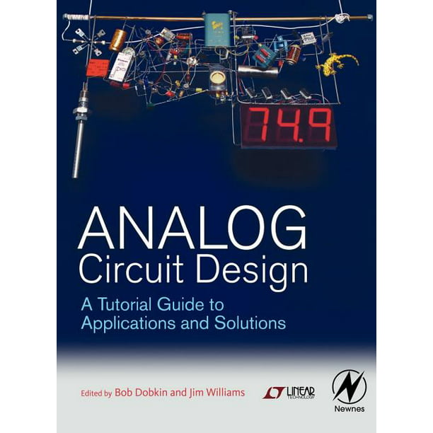
taqueso fucked around with this message at 20:34 on Dec 30, 2020 |
|
#
?
Dec 30, 2020 20:30
|
|


|
Yes, that's exactly the sort of thing I had in mind! No need to constrain the thread to just manufactured PCBs when there are so many cool hand-made circuit construction techniques too. Since I've mostly finished the work of producing a functioning release of the basic PNG->GRB software I've set my sights on mimicking another aesthetic: early-1980s through-hole logic boards. Since these are mostly just painful nests of routes I'm working on a tool to do the routing for me:  It also renders all of the traces in an appropriately-chunky-looking aesthetic by rendering everything on a 4x4 pixel grid then scaling it up with bi-linear filtering and thresholding. The images look like this before scaling:  taqueso posted:Ambrose, your post reminded me of the cover of this book (its from a series of 3ish books and they all have cool circuits on the covers iirc): You see book covers like that and you think, "wow that's a pretty circuit somebody built for that book cover". But it's just the way those guys worked. I don't know if they ever really got on board with simulation so they would just hack these things together. Bob Pease was known to say his favorite programming language was solder. This national treasure is Jim Williams's lab bench from when it was at the Computer History Museum in Mountain View (from https://www.flickr.com/photos/mightyohm/6926146703/in/set-72157629444825281): 
|
|
#
?
Dec 31, 2020 02:50
|
|
|
Good lord no wonder I love his work, he is clearly a kindred spirit  At my first job my boss would secretly be driven crazy by my "piles of poo poo" storage method but admitted he himself learned years ago that some people just work that way when he tried to clean up his father in law's area when he worked for him and got screamed at later. That job was a factory that made little light bulbs first for B-27s in WW2 and later supplied them to the space program and still filling orders for satellites. The production line was a bunch of old machinery with little weights dangling off pieces everywhere (sometimes like a couple paperclips) that tuned the machines just so. Mindblowing. I know they're laying out silicon here but I wonder what the program they're using is and if it's ancient enough to have the source available to try to pick out their routing algorithms? https://www.youtube.com/watch?v=tc4ROCJYbm0&t=1283s Edit: It sounds like he says at least one of the pieces is LGen or maybe Elgin but I can't find anything by that name. I wonder if it got renamed later or if I just am not hearing it correctly. Forseti fucked around with this message at 17:09 on Dec 31, 2020 |
|
#
?
Dec 31, 2020 17:02
|
|

|

|
| # ? Apr 25, 2024 13:01 |
|
|
Forseti posted:I know they're laying out silicon here but I wonder what the program they're using is and if it's ancient enough to have the source available to try to pick out their routing algorithms? Routing seems to be the fast part of this; it's the png->grb converter that's slow. Part of that is just that I took a class on physical design automation algorithms and I did not take any classes on graphics algorithms so I'm sure I'm doing that part the slowest way possible. I'm having way too much fun with this, though. I clearly need to turn it loose on a real circuit. It even did an OK job with this LED display matrix type thing (I can pretend the redundant vias are a feature): 
|
|
#
?
Dec 31, 2020 20:02
|
|